September 2026–present
Work in progress
Sending Data Through Lasers
Building a 638 nm optical link between two Raspberry Pis with six custom PCBs, from USB interfaces and laser drivers to mixed-signal, FPGA-based receivers.
- optics
- FPGA
- analog circuits
- PCBs
Link simulation
Hello world
—
Bit-aligned traces. TIA voltage is illustrative, on a relative scale.
Each node has a Raspberry Pi, USB interface, transmitter, and receiver. Two independent beams carry data in opposite directions.
Transmission is slowed for visibility. The simulation sends raw payload bits; the planned link uses 8b/10b coding and CRC-based retries, with a 50 Mbit/s line-rate target.
Overall architecture
The link is designed around two matching nodes. Each has a Raspberry Pi, a physical USB interface (PHY-A), a transmitter (TX-A), and an receiver (RX-A). Two separate beams carry data in opposite directions, allowing each node to transmit and receive simultaneously.
The Raspberry Pis run the host CLI software; the custom boards handle the optical link. An STM32F723-based USB interface buffers data between the Pi and the transmitter and receiver boards via USB 2.0 to the Pis. TX-A drives an HL63603TG laser diode from a serial input from the STM32. At the other end, RX-A converts the incoming light into a differential signal, with an iCE40UP5K FPGA intended to recover timing and decode the data before passing it back to the Pi through the STM32.
PCBs
Each node uses three boards: a USB interface, a transmitter, and a receiver. These models were exported from KiCad on September 8, 2026, including copper tracks, pads, vias, and silkscreen.
USB interface
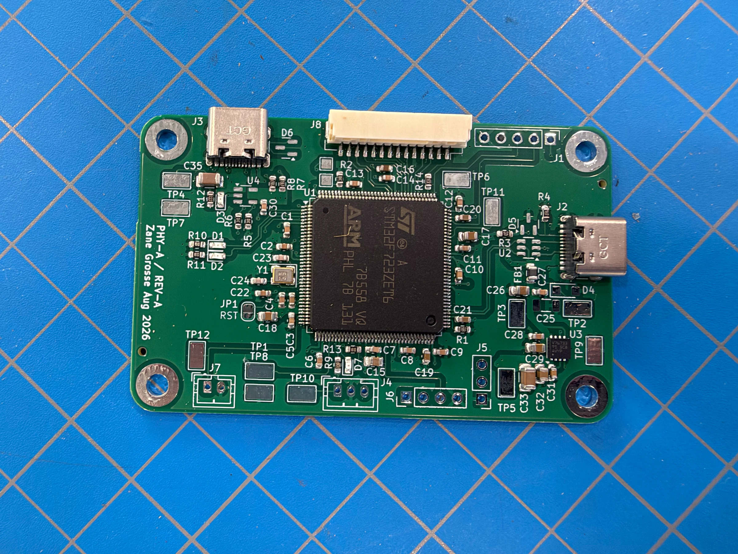
This board connects the Raspberry Pi to the optical hardware. It buffers outgoing data for TX-A and accepts recovered data from RX-A.
STM32F723 Handles USB communication and data between the host and the two TX/RX boards.
Board connections A serial data line feeds TX-A. A separate connection (the large 14 pin) brings decoded bytes and control signals back from RX-A.
Power and debug Local power handling, a programming header, and status indicators support bring up independently of the host software
Buffers data between the Raspberry Pi, transmitter, and receiver.
TX-A / transmitter
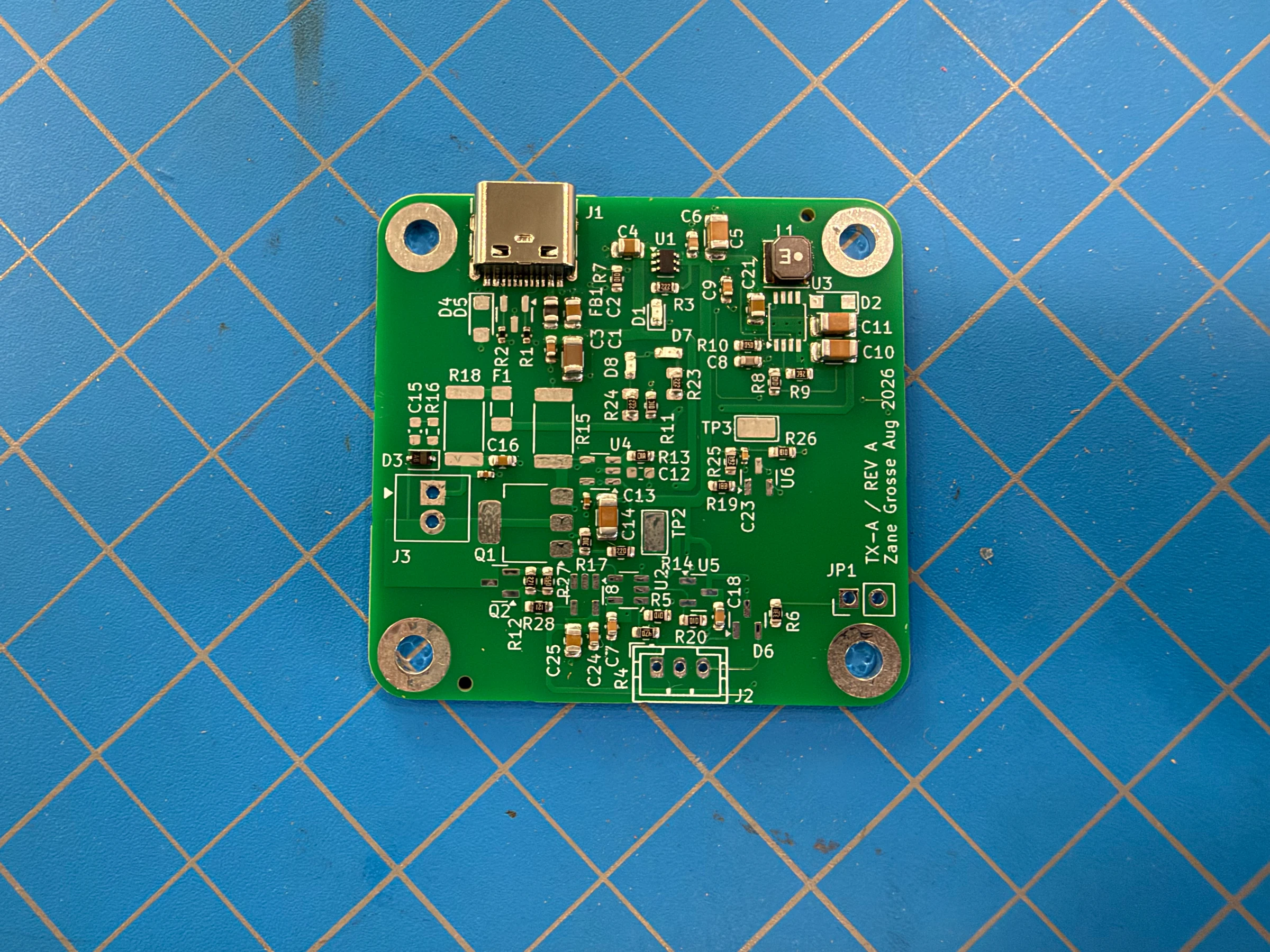
TX-A converts the incoming bit stream into changes in laser current. The laser is mounted separately from this board via screw terminal.
Current driver The analog driver sets the diode current, while the modulation path switches the optical output with the data.
Power and enable A TPS61085 boost converter supplies the driver, taking 5V (sourced upstream from Pi 5V peripheral line via USB) to 8V. Arming this rail requires both the physical jumper and the digital arm signal from the PHY board (PHY-A).
HL63603TG · 638 nm The external laser diode which creates the 638 nm light for carrying data between hosts.
The OPA356 compares the current-sense signal with the setpoint and drives the current-control stage.
RX-A / receiver
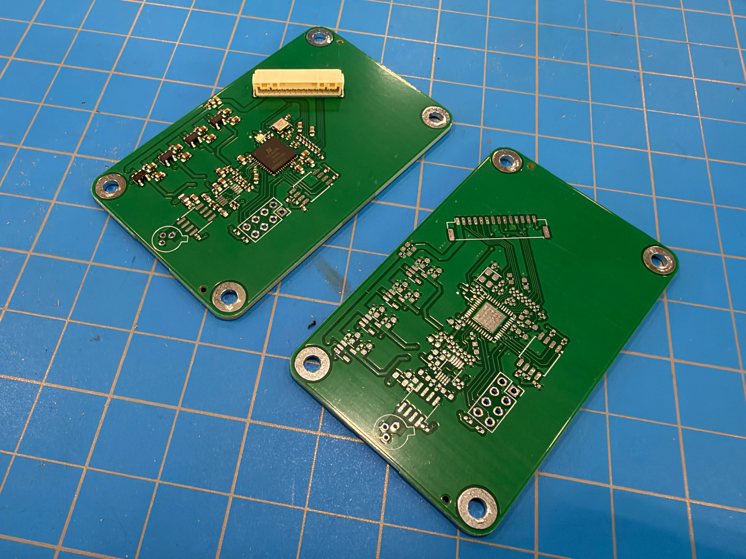
RX-A contains the optical front end and the FPGA. It turns incoming light into a differential signal that can be decoded and passed to the USB interface.
S5972 The photodiode produces a current in response to received light, chosen specifically for its response to 638 nm wavelength and balance of capacitance to surface area.
AD8015 → SY88803V The transimpedance amplifier converts that current to a voltage. The limiting amplifier conditions the signal for the digital stage.
iCE40UP5K The FPGA is intended to recover timing, decode the stream, and deliver recovered bytes to the USB interface. Programming done via SPI to external flash.
Converts incoming laser light into a small electrical current.
Mechanical layout
The mechanical assembly brings the Raspberry Pi, USB interface, transmitter, and receiver onto a shared sled. A common baseplate carries the board mounts, laser holder, and receiver optics above the 2040 rail.
These images were captured directly from the Fusion assembly on October 14, 2026. The close-ups show the receiver shroud and the laser mounting hardware. This is the current CAD layout; physical fit and optical alignment still need to be checked during assembly.
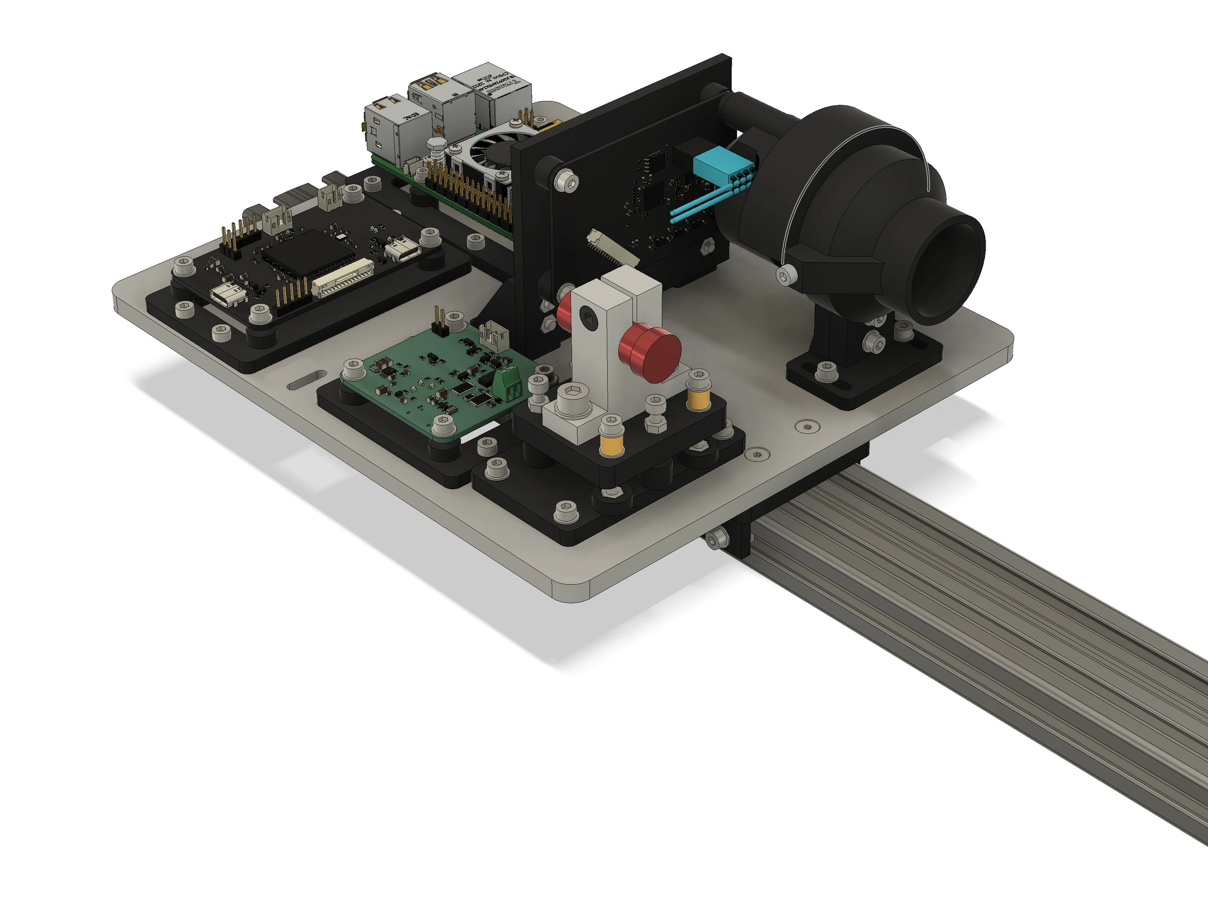
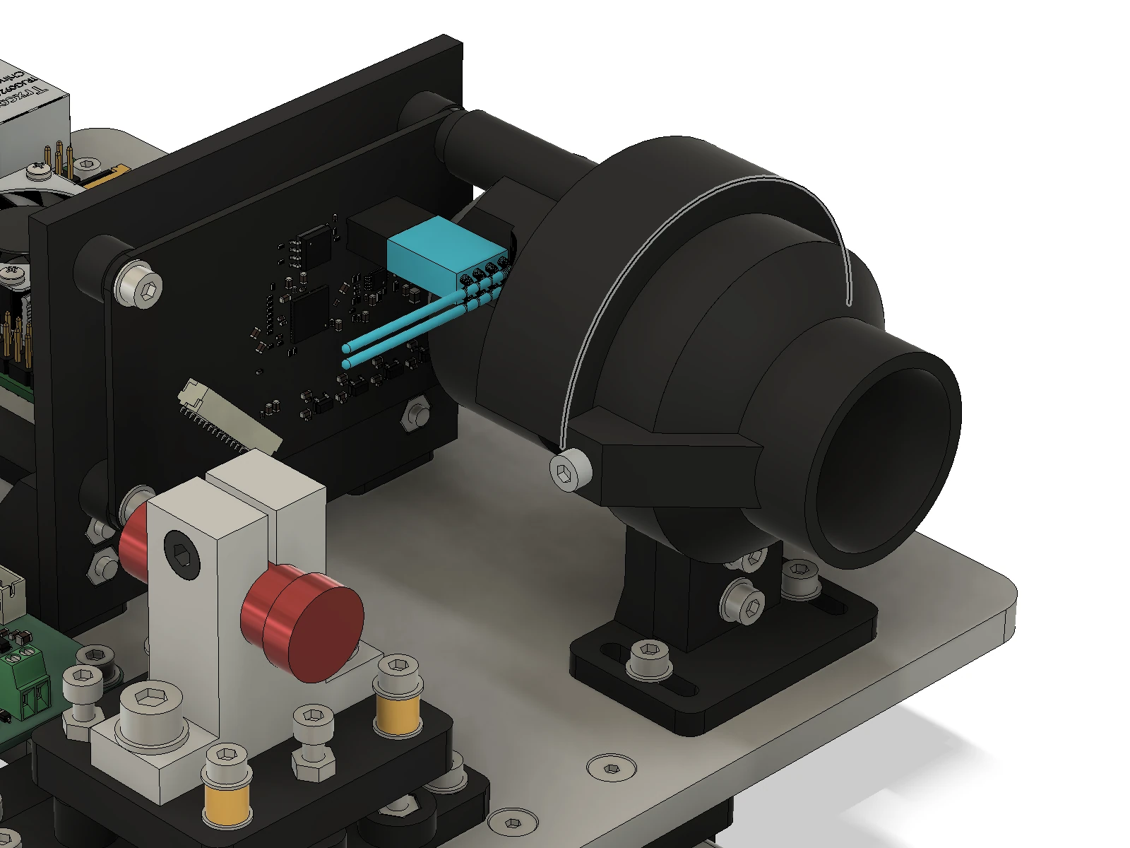
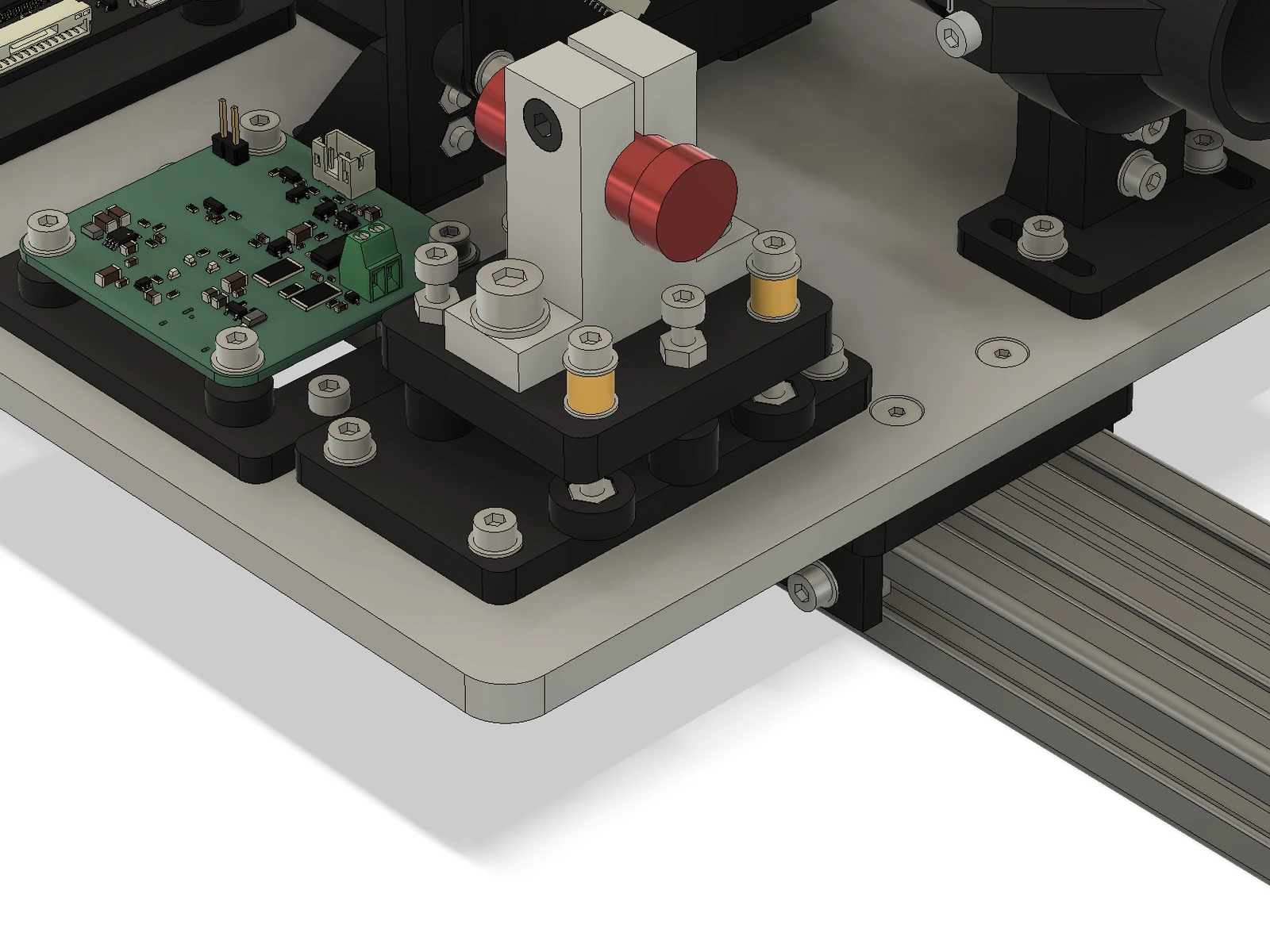
Explore the assembly
Rotate the sled to inspect the board carriers, receiver shroud, and laser mount. Select Full rail to see the complete assembly, or Reset to return to the sled. The STEP download contains the full assembly exported from Fusion.
Bring-up
Notes on initial power-up, board testing, and the first optical link.
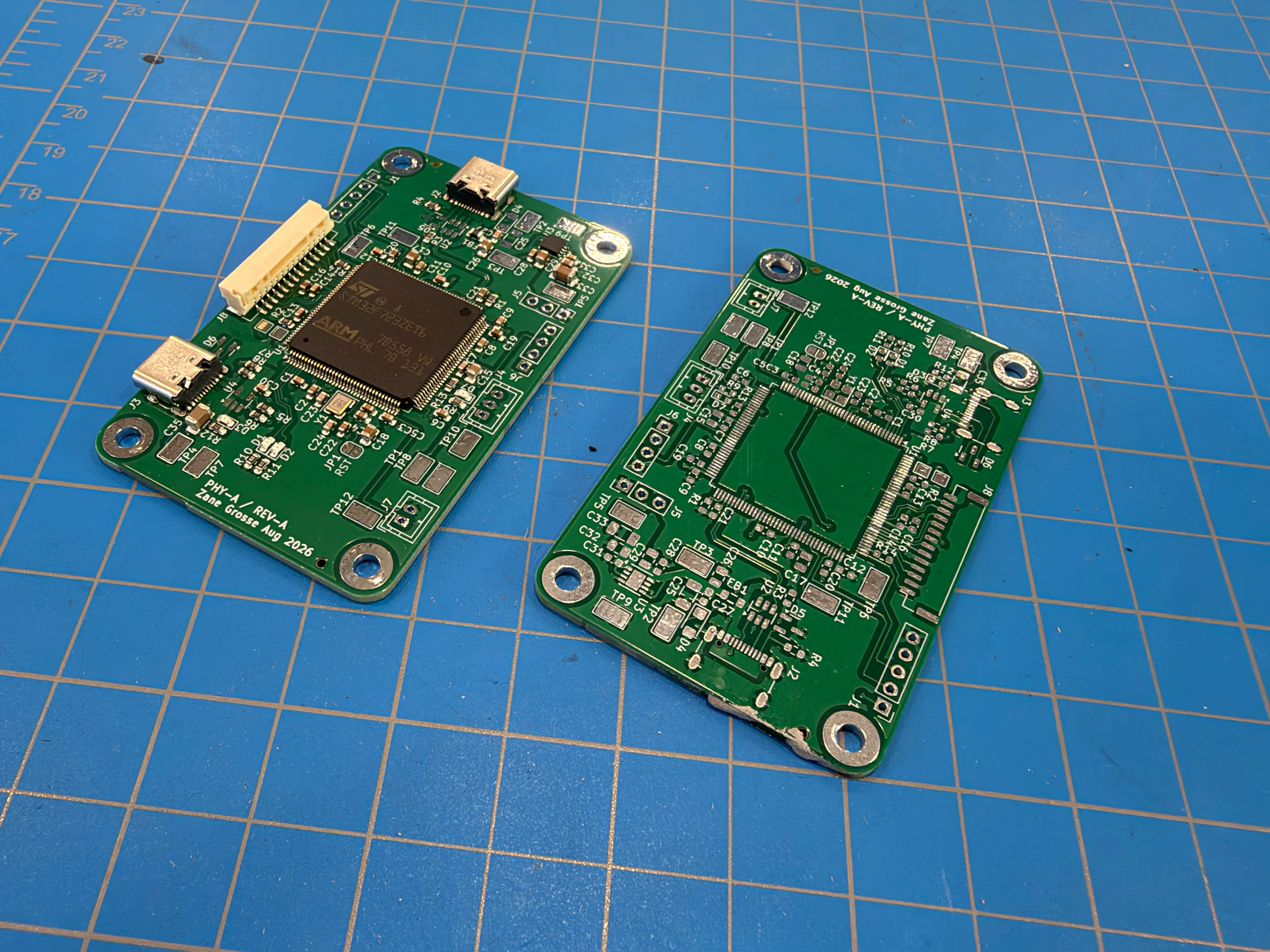
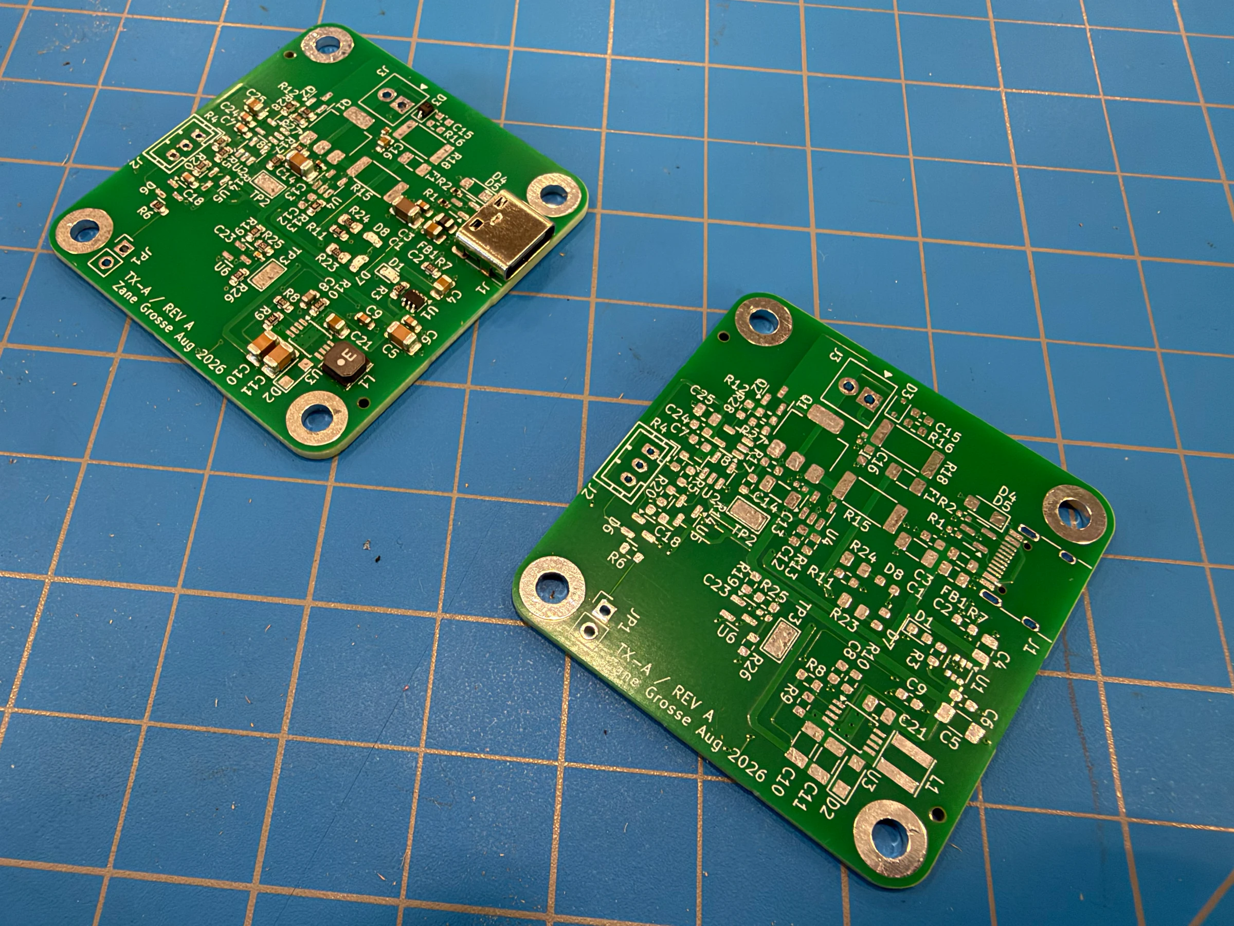
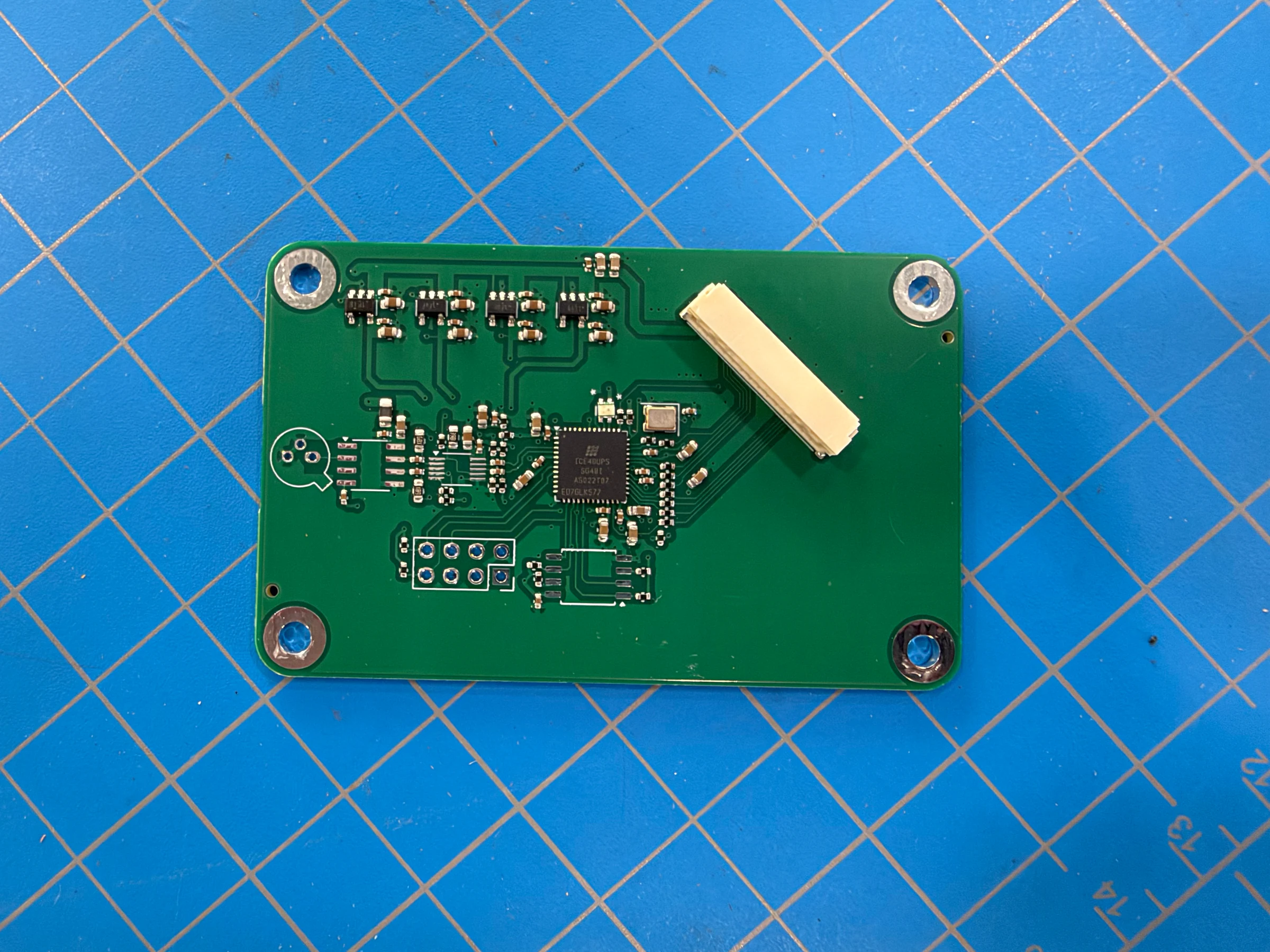
Boards as received
The USB interface, TX-A, and RX-A boards before manual population of the remaining components. The paired views show each board alongside an unpopulated PCB. Select a photo for a closer look.
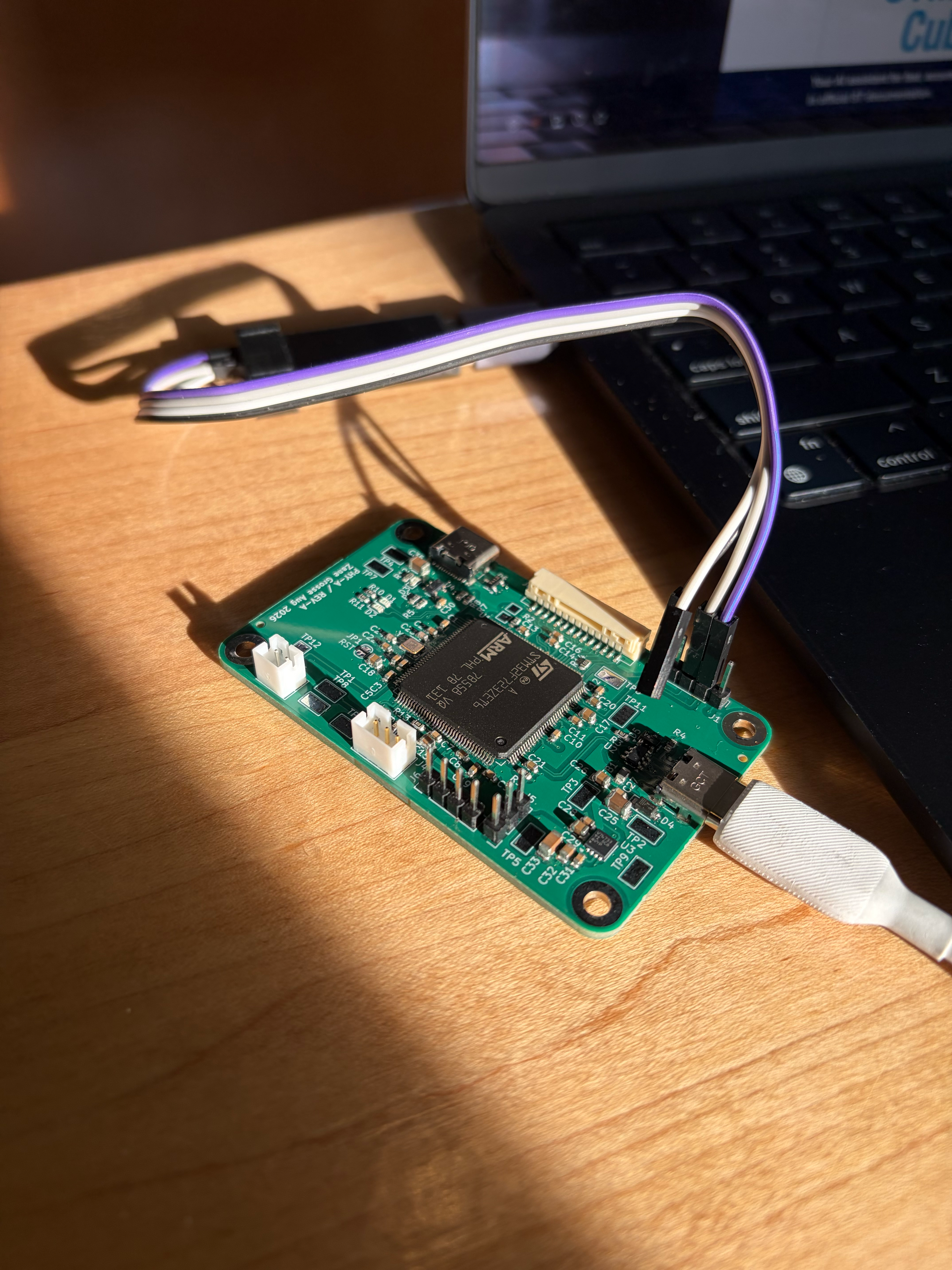
Power and first firmware
All power rails check out, and a simple test program has been flashed to the STM32F723. The clock and GPIO/control signals have also been verified.
TX-A / 8 V rail
The TPS61085 boosts the incoming 5 V supply to the nominal 8 V laser-driver rail on TX-A. This rail requires two arming conditions: the physical jumper must be fitted, and the PHY board (PHY-A) must assert its digital arm signal.
The first oscilloscope check shows a beautifully flat trace: 7.969 V average, with 32 mV peak-to-peak variation in this capture—about 0.40% of the measured rail voltage. The photo below records the steady-state rail, with the measurements transcribed underneath.
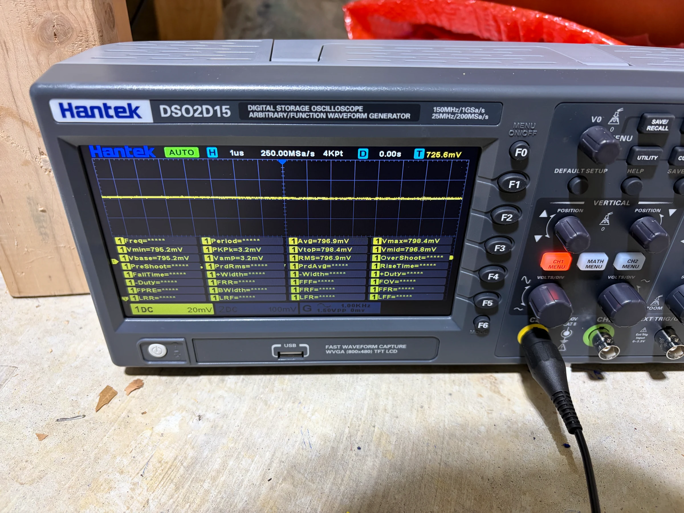
| Measurement | Scope display | Rail voltage (x10) |
|---|---|---|
| Average voltage | 796.9 mV | 7.969 V |
| Minimum voltage | 795.2 mV | 7.952 V |
| Maximum voltage | 798.4 mV | 7.984 V |
| Peak-to-peak variation | 3.2 mV | 32 mV |
| RMS voltage, including DC | 796.9 mV | 7.969 V |
| Mid-level voltage | 796.8 mV | 7.968 V |
Probe scaling: the probe was set to 10× while the scope channel was set to 1x, so voltage readouts are multiplied by ten in the rail-voltage column. Channel 1 is DC-coupled at a displayed 20 mV/div (200 mV/div at the rail), with a 1 us/div timebase and 250 MSa/s acquisition over a 4K-point record. The RMS reading includes the DC level; it is not an RMS ripple measurement.
The TPS61085 documentation from Texas Instruments is the boost convert used (5V to 8V). But arming is not done with the 61085's en pin, but rather, an upstream TPS22919DCKR that modulates the clean incoming 5V rail from a digital signal from PHY. (The armed 5V line is also controlled by this same digital signal for many peripherals)